MegaSquirt® Electronic Fuel Injection Computer - V1.01 Board Assembly Information
If you are looking for assembly instructions for a V3.0 main board, click here.
Follow the latest schematics on this site for assembling your MegaSquirt® PCB. There have been a few changes in the circuit to enhance the drive capability of the injector drivers. This document covers main board version V1.01.
The recommended order for assembly is the following: - First, install and solder the 9 pin and 37-pin connectors. Next, install the 40-pin processor socket (align the notch in the socket to correspond with the notch on the silk screen).
- Next, install all components on the schematic under the "MegaSquirt - Power" schematic page. Next, hook up the stimulator board (or an external power source into the V12RAW and ground) and check for +5 volts at to 40-pin processor socket (+5 at pins 1, 20, 31, using ground at pins 2, 19, and 32 - check all combinations).
- Now, install all components on the "Megasquirt - Connector" schematic page, which includes the RS-232 driver (the MAX232 part solders down directly on the board). Now, plug in the MC68HC908GP32 processor into the 40-pin socket, and plug up a 9-pin serial cable to your PC which has the PC Configurator program. Apply +12 volts to the board (using the stimulator or external power), and fire up the PC Configurator program, and enter the "Runtime Display" option. You should see the "Seconds" field count up every second (it will roll over at count 255 to zero) - if you see this then the processor is running! If not then check polarity of components, solder joints, PC Configurator, etc. Note that none of the stimulator controls will operate at this point - you are using the stimulator to apply power only.
- Now, install all of the components on the "MegaSquirt - Inputs" page. Now, connect everything up as in the step above, and all of the input signals should operate (TPS, MAP, O2, coolant, air temp) from the stimulator, and show up on the runtime screen. Debug individual channels as required.
- Next, install all of the components on the "MegaSquirt - Outputs" page. Hook up the stimulator, and verify that the LEDs operate for each channel. You can change values from the PC Configurator and see the effects on the stimulator.
- Finally, install the LEDs and put everything in the case (described below). Bolt on the car and go.
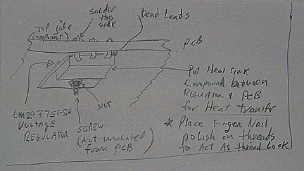
All components mount of the silk-screen side of the board (top), with the exception of the voltage regulator IC (part U5), which mounts on the underside of the PCB (solder side). The voltage regulator lays flat on the backside of the board, mounted with a 8-32 x 1-1/4 bolt and nut - no insulating mica spacer is needed (the tab is at ground potential). Use heat sink compound on the tab surface to the PCB for heat conduction (available at electronics stores like Radio Shack). The three leads are bent at a 90-degree angle and pass thru the board, and the leads are soldered on the top side of the board.
Do not install diodes D1, D2, D3 and D4 (all 5.1 volt Zener diodes). Motorola has confirmed that the MC68HC908GP32 has protection diodes on the inputs of the Analog-to-Digital Converter channels, and these are sufficient to prevent voltage spikes from damaging the processor or ADC channels, and the added protection from external diodes is not needed. Also, there can be tolerance issues with some Zener diode which may limit the full-scale range of the ADC channels, so it is strongly recommended to leave these out..
The metal can 2N2222A transistors should NOT be mounted all the way (flush) down on the board surface (Q3, Q5, Q9, Q10, Q11), to prevent shorting of the traces below the device. Space the transistors something like 1/8" (3 mm) from the board surface, and solder. Also, the two inductors should also be mounted spaced off of the board (1/16") to prevent shorts, and well as D6 and D10 (33 volt Zener diodes) for adequate cooling.
In the group purchase, the processor chips which are programmed for the turbo MAP (MPX4250) has a handwritten "T" on the top, made with a red felt-tip pen. The processors for the MPX4115 MAP sensors have no markings. For those who have both types of boards, make sure you match up the right processor with the right MAP.
The capacitor C17 can be confusing on the PCB footprint. The capacitors go through the outer two holes - the center hole is a via for connecting the two PCB sides - you leave the center hole alone. Look at other capacitors nearby to see what I mean.
Follow the silk-screening to determine part location. All integrated circuits have outlines on the silk screen denoting orientation, and pin #1 is indicated by a square PCB pad instead of round. Similarly, the positive terminal of electrolytic capacitors are indicated by the square pad, and pin #1 of the MAP sensor is also square. Diodes are oriented with the band corresponding to the band on the silk screen.
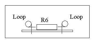
The resistor R6 (just to the left of the processor) has a special mode. By placing a jumper wire across this resistor (denoted on the PCB by the label "BOOT") the ECU will enter Bootloader Mode upon power-up - this is used for code updates. For normal operation, this resistor is left un-jumpered. - To ease the placement of the jumper across this resistor, it is recommended that the leads be bent to form a small circle right before entry into the PCB hole. By doing this, one can easily attach a jumper wire.
- For those using their unit for development and plan to enter Bootloader Mode on a regular basis, one may solder small wires to this resistor which connect to a SPDT switch which is mounted somewhere on the case. By closing the switch contacts, one can enter bootloader mode, otherwise they can run the unit in normal mode with the switch open.
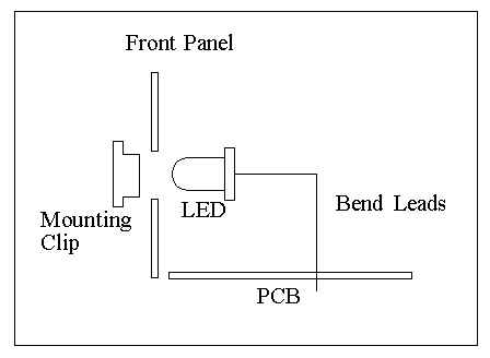
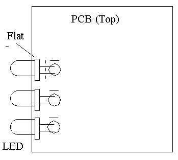
The three LEDs mount on the front panel (using the LED mounting clips) and the leads are bent at 90 degrees to enter the PCB. The LED has a flat side along the bottom - this indicates the cathode end. On the circuit board, the silk screen for the LED is a circle - notice that right above the circle there is a small line (or dash) - this indicates the cathode terminal, the lead of the LED which is closest to the flat side goes here. - It is recommended that the LEDs be installed after the PCB is installed in the case. Drill out the front panel, insert the LEDs using the mounting clips, and slide the PCB in the case. Bend the leads of the LED down 90 degrees and put into the correct PCB holes, and solder from the top while the board is still in the case.
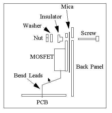
The two MOSFET injector drivers use the rear panel for mounting and heat sink. The MOSFET tabs are "hot" and must be electrically-insulated from the back panel. Use the mica insulating spacer, heat sink compound, and the plastic spacer - study the diagram below for assembly. Make sure that the hole in the rear panel is deburred to prevent the panel from shorting to the tab. After assembly, use an ohmmeter to check that there is an infinite resistance between the tab and the rear panel. - In addition, the leads must be bent to enter the holes on the PCB. Once again, study the diagram. And, like the LED mounting, the best method is to mount the MOSFET on the back panel, mount the PCB in the case, and then mount the back panel to the case while bending the leads into the proper holes. Take your time and do this step right - it is the most difficult part of the assembly.
- Also, make sure that the tab of the MOSFETs so not touch the sides or the top of the case - if they do then the driver will short out to the case. Grind the rail of the case, if required, to ensure that the tabs do not touch the case (other than where the mica insulating washer is installed).
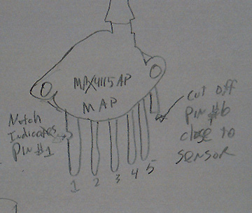
The Manifold Absolute Pressure (MAP) sensor is mounted on the V1.01 PC board straight up (the port is up). The lid of the case (top half) is drilled to allow the port to stick through. A rubber vacuum hose fits over the barb (3/32") so the hole must be big enough for the vacuum line to pass - this also acts to support the MAP sensor from the top. - You will notice that there are six leads from the MAP sensor, but only 5 holes in the PCB. Yes, this is a goof on my part in the PCB pad assignment which I have never fixed. So, what you have to do is clip off pin #6 from the package. Pin #1 is denoted by a half circle" notch" in the lead - the lead on the other end is pin #6. See the diagram below.
- On the PCB, pin #1 is the square pad (near the bottom edge of the PCB).